Subtotal ₹8,300.00


This project presents a new single-phase switched coupled-inductor dc–ac inverter featuring higher voltage gain than the existing single-phase qZ-source and semi-Z-source inverters. Similar to the single-phase qZ-source and semi-Z-source inverters, the proposed inverter also has common grounds between the dc input and ac output voltages, which is beneficial especially for photovoltaic inverter systems. The inverter volume and maximum current flowing can be reduced significantly through the coupling of all inductors
Nowadays, there is an increasing demand for low-cost single-phase dc–ac inverters in many applications such as photovoltaic (PV), fuel cell, and battery powered systems. The conventional method shows the well-known full-bridge (FB) inverter referred to as buck inverter. In this method, the inverter output voltage (vo) cannot be greater than input voltage (Vin ). This may result in large leakage current in applications such as transformer-less grid-tied PV inverter, which will cause safety and electromagnetic interference problem. In order to overcome the disadvantages of the conventional inverters, a large number of single-stage inverters are proposed.
A single-phase switched-coupled-inductor dc– ac inverter is proposed. Similar to the TSTS (Three switch and three state)-ZSI(Z-source inverters), the proposed inverter can obtain higher voltage gain and maintains same ground between Vin and vo. The proposed inverter also requires three active switches, but all the inductors in the circuit can be coupled together, which will lead to more compact and cost effective solution than the TSTS-ZSI. In addition, the switch signal generation is relatively simpler than the TSTS-ZSI.
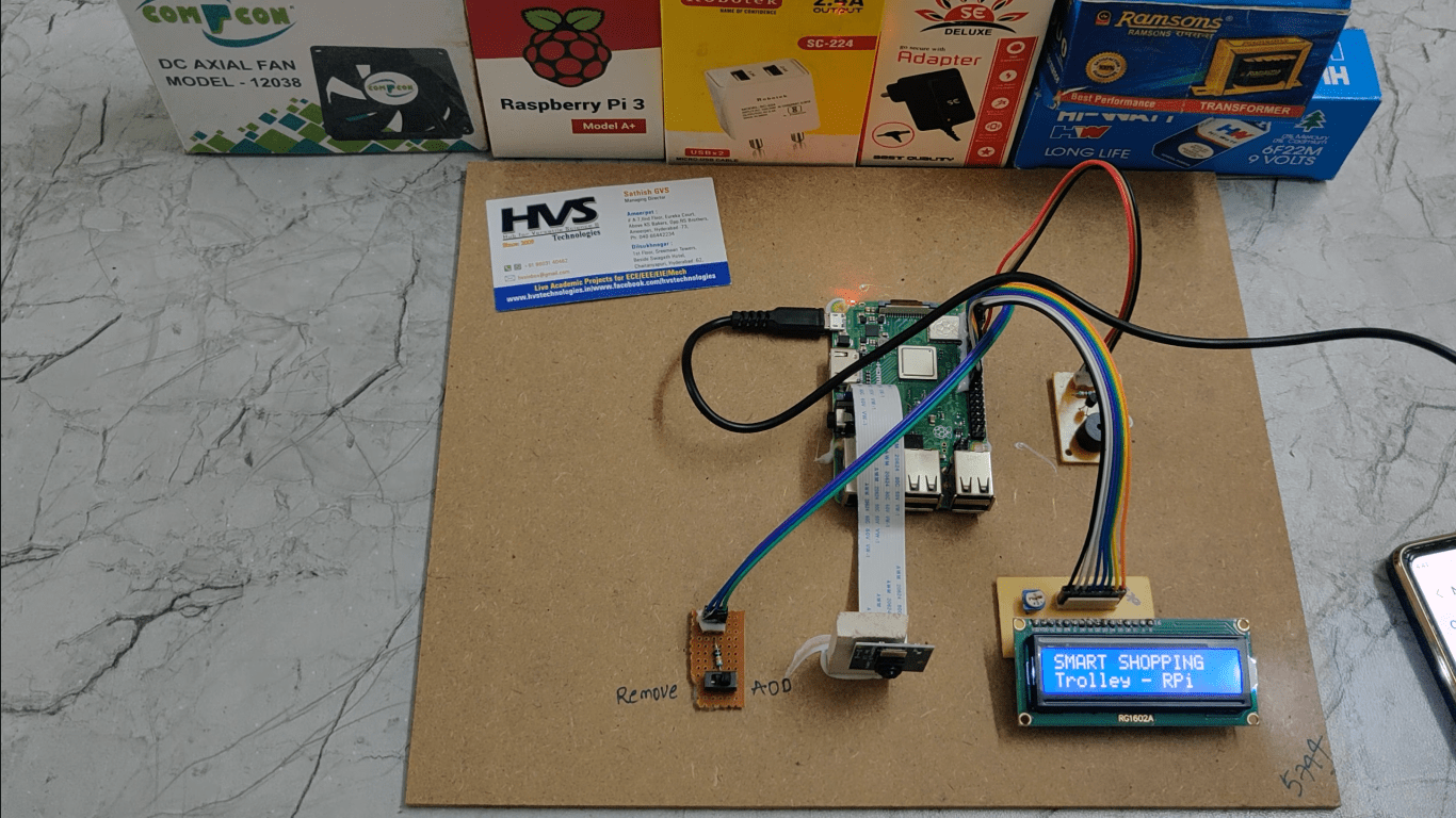
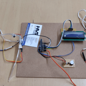
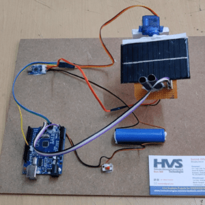
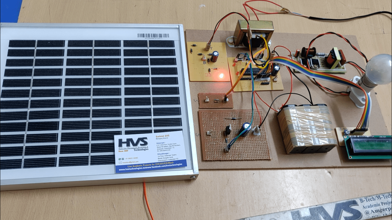
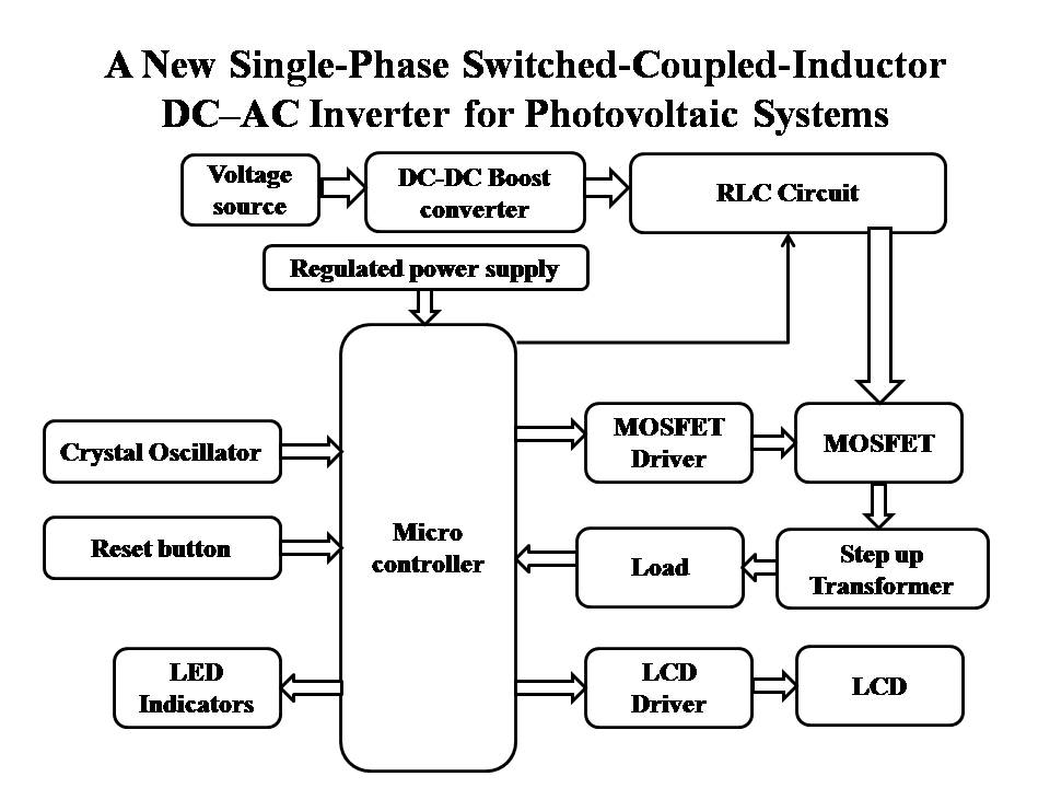
Major blocks present in this project:
 video:
- Regulated power supply
- DC-DC Boost converter.
- RLC Circuit.
- Micro controller.
- MOSFET Driver.
- MOSFET
- Step up transformer.
- Load
- LCD
- Crystal Oscillator
- Reset
- PIC-C compiler for Embedded C programming.
- PIC kit 2 programmer for dumping code into Micro controller.
- Express SCH for Circuit design.
 video: