No products in the cart.


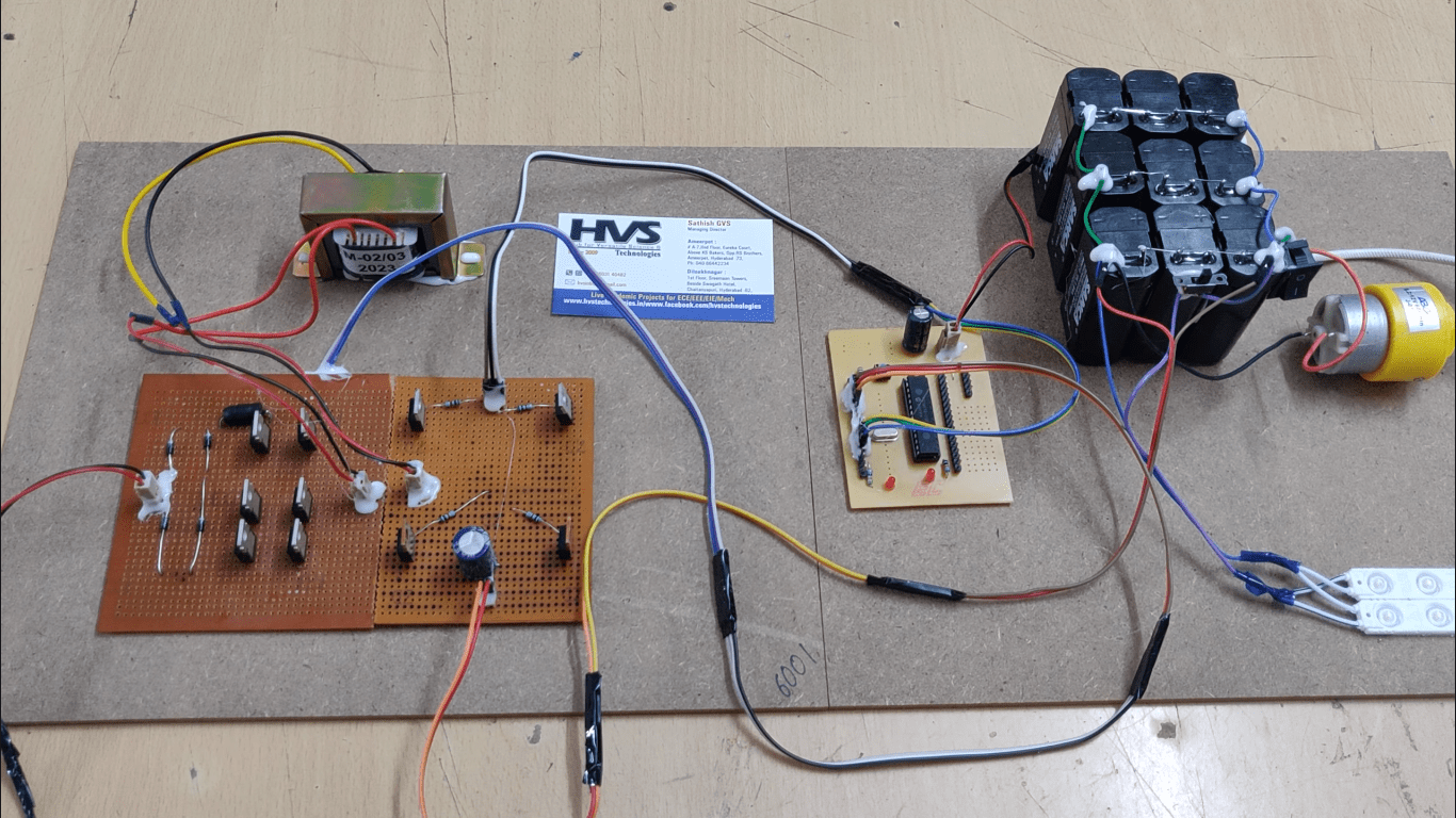
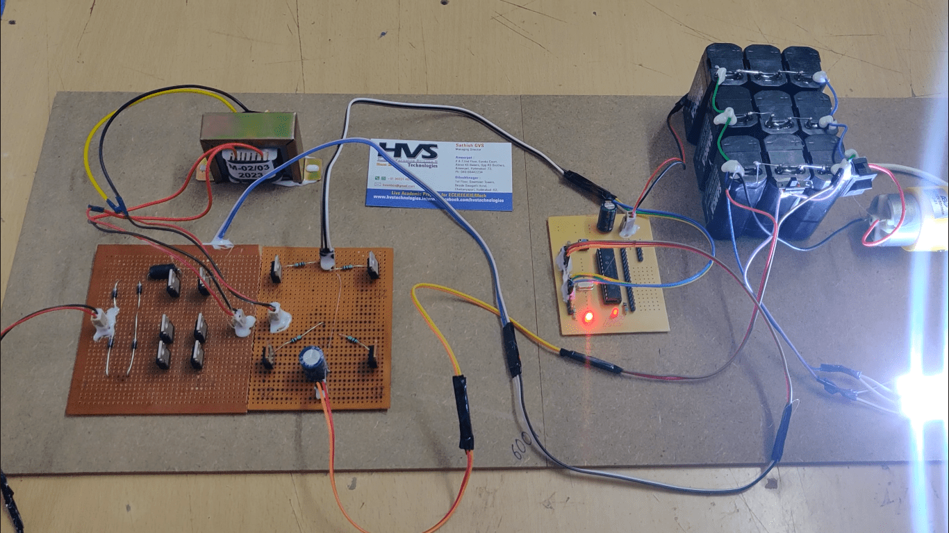
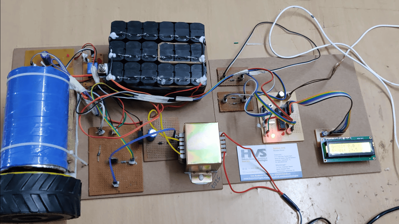
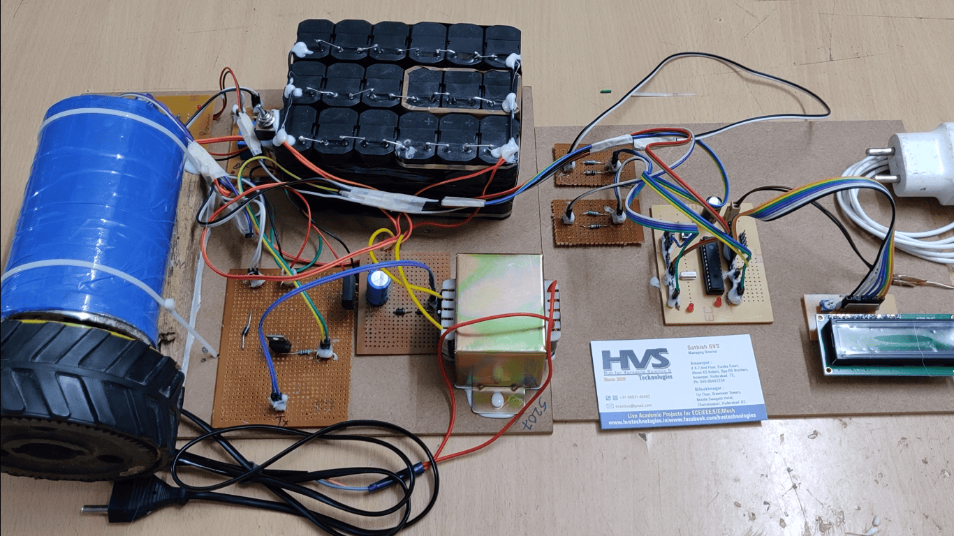
The primary objective of this project is to present an isolated single-stage On Board Charger (OBC) without an intermediate DC-Link. Regarding the current source topology proposed for the EV OBC, it does not require external clamp circuits, and only two inverter transistors should feature reverse voltage blocking capability. The OBC topology shown utilizes two magnetic components, providing the soft-switching for the transistors in the full input voltage range and a constant switching frequency regardless of converter gain requirements. The circulating energy required for soft-switching is regulated based on the instantaneous value of the input current. This feature also reduces the conduction losses in the converter due to minimized circulation energy, resulting from input voltage variation or light load operating conditions. The lossless snubber capacitors are applied across secondary devices to reduce the switching dv/dt and turn-off losses.
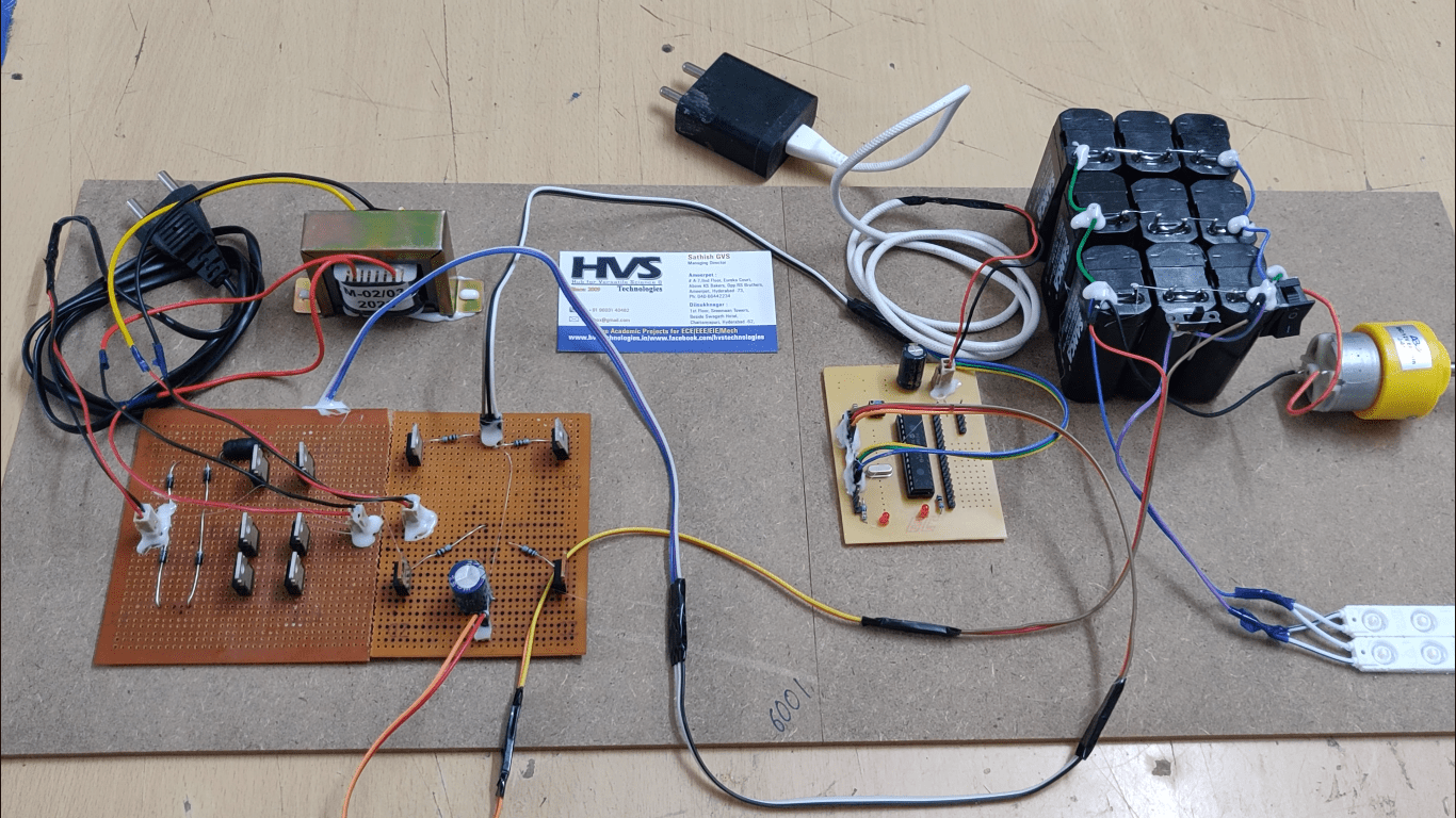
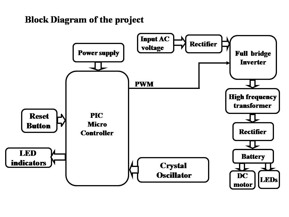
The grid voltage VgV_g is rectified to unipolar pulsating voltage VpV_p utilizing the diode bridge D1D_1-D4D_4. The input rectifier could consist of passive diodes for unidirectional charging applications or active switches for bidirectional energy flow. The following analysis assumes that the components are ideal and lossless. The effect of magnetizing inductance of the transformer TXT_X is not taken into account, as it is not utilized in the proposed modulation method. The input unipolar pulsating current IpI_p flows through the inductor LinL_{in} that provides energy storage for boost operation and acts as the input filter of the converter. Further, the energy is transferred to the load, utilizing a full-bridge inverter, a high-frequency transformer, and a rectifier.
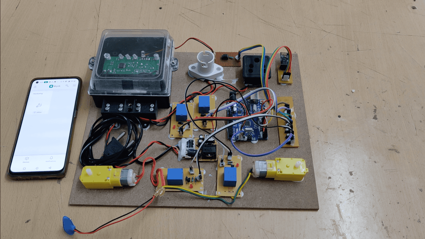
To ensure efficient control, monitoring, and protection of the charger system, a PIC microcontroller is integrated into the design. The PIC microcontroller is responsible for generating switching signals for the inverter, regulating the charging process, monitoring input/output voltages and currents, and providing protection against overvoltage, overcurrent, and thermal faults. Its programmable nature and real-time processing capability make it a suitable choice for implementing control algorithms, thereby enhancing the overall reliability and performance of the proposed single-stage OBC.
The major features of this project are:- To design an isolated single-stage On Board charger without an intermediate DC-Link.
- Use of current source topology.
- Grid Voltage
- Rectifier
- Full Bridge Inverter
- High Frequency Transformer
- Battery
- Pic Micro controller
 video: